64Kbit dual-port SRAM for shared-memory designs
Its 15 ns access time and 15 ns write cycle time let it keep pace with moderate-speed microcontrollers and DSPs without inserting wait states on a 5 V bus. The dual-port architecture gives each port its own address, data, and control lines, so a processor and a DMA controller — or two processors — can read or write the same location concurrently, with on-chip arbitration handling collisions.
15 ns access — bus timing margin
For a processor running at 33 MHz (30 ns cycle), this part leaves about 15 ns of bus timing margin after address decode and setup — comfortable for a glue-logic interface without a fast-page or pipelined memory controller. If your system clock is faster than 40 MHz, you will need to add wait states or look at a 12 ns or 10 ns dual-port SRAM.
Industrial temperature and 5 V supply
If your new design has moved to 3.3 V or 1.8 V core logic, this SRAM will need a level translator or a separate 5 V rail.
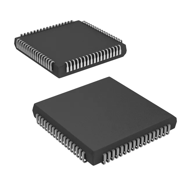
68-PLCC package — hand-solderable and rework-friendly
The 68-lead PLCC with J-leads (24.23 mm square body) is a surface-mount package that can still be hand-soldered with a fine-tip iron or hot-air rework station. The J-lead form gives a visual solder-joint inspection and is easier to desolder than a QFP. The PLCC socket is also available for prototyping or field-replacement scenarios. No exposed thermal pad — the package relies on the leads for heat conduction, so keep air flow across the part if dissipation is significant.
No last-time-buy window is open from the factory.