What the 15 ns access time means for your bus
The CY7C144-15JXCT is a 64Kbit dual-port asynchronous SRAM organized as 8K x 8, with a 15 ns access time that sets the window for the memory controller to latch data on the parallel bus. At 15 ns, the part keeps pace with most 8-bit microcontrollers running at 20-25 MHz without wait states, but a faster controller will need to insert cycles or switch to a pipelined memory. Dual-port architecture means two independent devices can read or write to the same memory location simultaneously — useful in shared-memory designs like a dual-processor system or a bridge between a DSP and a host controller. The asynchronous interface eliminates the need for a clock on the memory side, simplifying the PCB layout.
68-PLCC package and reflow reality
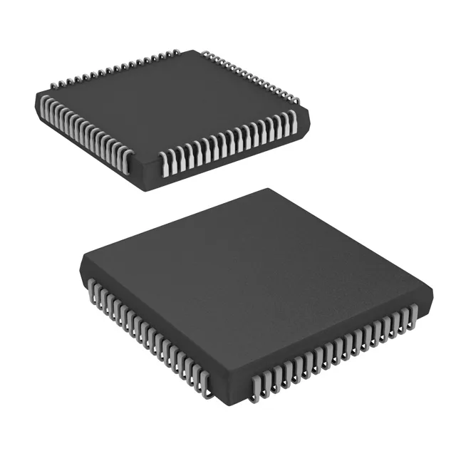
The tape-and-reel packaging suits automated assembly lines. The 68-PLCC footprint is standard — the JEDEC MO-047 outline matches most land patterns, so no custom pad geometry is needed.
For a BOM that already uses this part, the 15 ns access time, 5V supply, and 68-PLCC package are the binding constraints for any replacement. A functionally equivalent dual-port SRAM from another vendor (e.g., IDT or Renesas) will likely require a different package or supply voltage — a board spin or socket adapter may be needed.
Supply voltage and temperature grade
Operates from 4.5V to 5.5V, which is the classic 5V logic rail — compatible with legacy 5V microcontrollers, CPLDs, and ASICs. The write cycle time matches the read access time at 15 ns, so the bus turnaround is symmetric — no extra dead cycles needed between read and write operations.