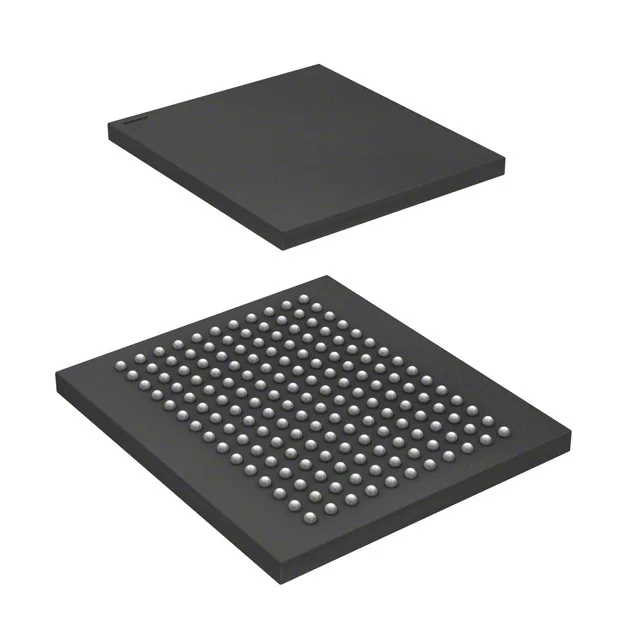
The CY7C1426AV18-167BZXC is officially marked Obsolete by Infineon Technologies. For a BOM line that still calls out this exact part, the procurement path is quoted-to-order against the RFQ — availability and pricing confirmed at quote time, no stock-holding claim.
36 Mbit QDR II — 167 MHz clock, 1.7–1.9 V supply
This is a 36 Mbit Quad Data Rate (QDR II) synchronous SRAM, organized as 4 M x 9 bits. The 167 MHz clock delivers a peak bandwidth of 334 million transfers per second on the read and write ports simultaneously — the QDR II architecture separates read and write buses so a single device can sustain full-duplex traffic without bus-turnaround dead cycles. Supply voltage range is 1.7 V to 1.9 V, which places it in the 1.8 V nominal core-logic family. The parallel memory interface means the address and data buses are shared with the controller — layout must match the trace-length constraints for a 167 MHz bus.
165-FBGA — rework reality
Housed in a 165-ball FBGA (15 x 17 mm body, 1.0 mm ball pitch). The package is surface-mount only — no socket option. The supplier device package is 165-FBGA (15x17) — confirm the PCB footprint matches the JEDEC MO-216 standard for this ball map before committing the layout.
This is the standard indoor/office-grade envelope — not suitable for extended industrial or automotive ambient without active cooling or derating.