36 Mbit DDR II SRAM — 300 MHz, 2M x 18
It operates at a 300 MHz clock frequency, delivering high-bandwidth data transfers on both clock edges through a parallel interface. This part is designed for applications requiring fast, predictable memory access with low latency — typically network packet buffers, telecom line cards, and high-end test equipment where the DDR II protocol provides back-to-back read/write throughput without dead cycles.
The 300 MHz clock rate, combined with DDR II signaling, yields an effective data rate of 600 million transfers per second on the 18-bit data bus. For a system architect, this translates to a peak bandwidth of roughly 1.35 GB/s (600 MT/s × 18 bits ÷ 8). The synchronous interface simplifies timing closure in high-speed designs, but the 165-ball FBGA layout demands careful PCB stack-up and signal integrity work — trace length matching on the 18 data lines plus address and control becomes non-trivial above 200 MHz.
There is no direct drop-in replacement from the manufacturer; any substitution requires a pin-compatible and timing-compatible evaluation against the original design.
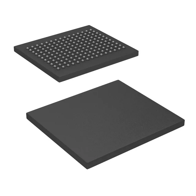
Housed in a 165-ball FBGA (15x17 mm) package, this is a surface-mount BGA that requires reflow soldering and X-ray inspection for void detection. The supply voltage range is 1.7V to 1.9V, typical for low-voltage high-speed SRAM cores; the 1.8V nominal rail must be clean, as ripple directly eats into timing margin at 300 MHz.