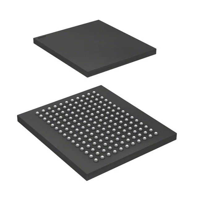
The Infineon CY7C1418BV18-267BZXC is a 36Mbit synchronous DDR-II SRAM organized as 2M x 18, clocked at 267 MHz. The 1.7–1.9 V core supply aligns with 1.8 V nominal logic families common in high-speed SRAM designs. The 165-FBGA (15x17 mm) package carries 165 balls — fine-pitch BGA that demands controlled impedance routing and a multilayer PCB with via-in-pad capability if you are routing all 18 data bits plus address at 267 MHz.
267 MHz clock — the throughput decision
At 267 MHz the DDR-II interface transfers data on both clock edges, so the effective data rate is 534 MT/s per pin. For a 2M x 18 part that means roughly 9.6 Gbit/s aggregate bandwidth on the data bus. That is the tier you spec when a FIFO depth of 2M words and sustained read-write throughput matters more than density — think packet buffers in a 10 GbE switch or waveform memory in a high-speed AWG. If the board sees an industrial floor or outdoor cabinet, you need the industrial-grade variant in the same family.
Infineon lists the CY7C1418BV18-267BZXC as Obsolete. That means the part is no longer manufactured and is not available through the factory channel. If you are qualifying a replacement, look at other 36Mbit DDR-II SRAMs in the 165-ball FBGA footprint with the same 1.8 V supply and 267 MHz speed grade. Pin compatibility across the Cypress/Infineon DDR-II family is common within the same density and package, but verify the ball map against your layout — the datasheet is the final authority.