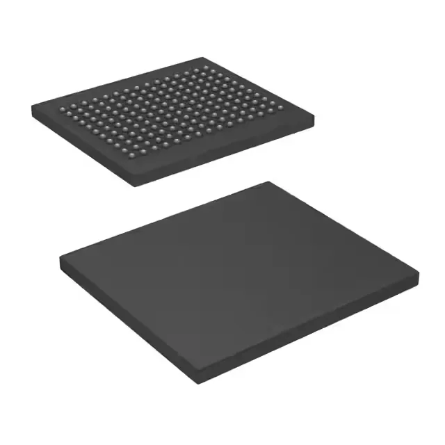
Infineon Technologies CY7C1415BV18-250BZC — Memory (DRAM / SRAM / Flash / EEPROM)

Cypress CY7C1415BV18-250BZC QDR II SRAM, 36Mbit, 250 MHz

MPNCY7C1415BV18-250BZC
Obsolete

Cypress CY7C1415BV18-250BZC, QDR II synchronous SRAM, 36Mbit (1M x 36), 250 MHz clock, 1.7V–1.9V supply, 165-ball FBGA (15x17 mm), 0°C to 70°C.

$45.3500Ref. price · indicative, final on quote
StockContact for availability
MOQ1 pcs
  • 100% new & originalTraceable channels only — no refurbs, no pulls, no remarked parts.
  • Date & lot codes on quoteStated per line before you commit; label photos on request.
  • MSL-compliant ESD packingMoisture-sealed bags with indicator cards; reels photo-verified.
  • PayPal buyer protectionPay by T/T, PayPal or Payoneer — card payments covered end to end.

Specifications

CY7C1415BV18-250BZC Technical Specifications
ParameterValue
Memory typeVolatile
Mounting typeSurface Mount
Voltage1.7V ~ 1.9V
Frequency250 MHz
Memory interfaceParallel
Operating temperature0°C~70°C(TA)
PackageTray
TechnologySRAM - Synchronous, QDR II
Memory size36Mbit
Memory formatSRAM
Case165-LBGA
Memory organization1M x 36

Product details

The CY7C1415BV18-250BZC is a 36Mbit synchronous SRAM using QDR II architecture — separate read and write ports, each running at 250 MHz. Organized as 1M x 36, it operates on a 1.7V–1.9V supply.

250 MHz clock — what it means for the bus

The 250 MHz clock rate on both ports allows a new read and a new write every cycle. This eliminates bus-turnaround dead cycles.

36Mbit density and 1M x 36 organization

The 1M x 36 organization is a natural fit for 36-bit wide data paths common in networking ASICs and FPGA-based packet processors. Each access delivers 36 bits in parallel, matching the width of a typical MAC or DSP datapath without needing external muxing. The 36Mbit capacity is sized for moderate-size lookup tables, packet buffers, or coefficient storage — enough for a 10G Ethernet line card's FIFO, but not for deep frame buffering.

Temperature grade and environment

Rated for 0°C to 70°C ambient, this is a commercial-temperature device. It belongs in indoor, temperature-controlled equipment — server rooms, telecom central offices, lab instrumentation — not in outdoor cabinets, engine bays, or factory floors where ambient can exceed 70°C. The 165-ball FBGA (15x17 mm) package requires a controlled reflow profile and X-ray inspection for voiding under the BGA.

Lifecycle and sourcing reality

The CY7C1415BV18-250BZC is officially marked obsolete by Cypress (now Infineon). No last-time-buy window remains open. For a BOM line that needs this exact order code, the only channel is the independent surplus and broker market. We source and quote to order against an RFQ — availability and current pricing are confirmed at quote time. There is no official pin-compatible successor from Infineon; any replacement would require a board respin and timing revalidation.

Frequently asked questions

What is the closest pin-compatible alternative to CY7C1415BV18-250BZC?

No official pin-compatible replacement is listed by Infineon. Any alternative would require a board redesign and timing revalidation. Check the QDR II SRAM family from other vendors (e.g., Renesas, GSI Technology) for similar 36Mbit, 250 MHz parts in 165-FBGA, but verify pinout and timing parameters against your design.

What package does CY7C1415BV18-250BZC use?

It comes in a 165-ball LBGA (also designated 165-FBGA, 15x17 mm body). Surface-mount, fine-pitch BGA requiring controlled reflow and X-ray inspection.

What is the technology of CY7C1415BV18-250BZC?

It is a synchronous QDR II SRAM — Quad Data Rate, second generation. Separate read and write ports eliminate bus-turnaround dead cycles, achieving 250 MHz operation on each port.