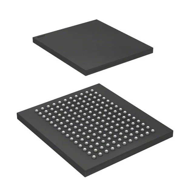
36Mbit QDR-II SRAM at 250 MHz — the bandwidth driver
The CY7C1415AV18-250BZCT is a 36Mbit synchronous SRAM using the QDR-II architecture — separate read and write ports running concurrently on each clock edge eliminate the bus-turnaround dead cycles that cut throughput on conventional shared-bus SRAM. At 250 MHz the device delivers a peak data rate of 1 GB/s on a 36-bit word (1M × 36 organization), which fits network processor look-up tables, deep packet buffers, and high-speed line-card memory where latency matters more than density. The 1.7–1.9 V core supply is a tight window — the board-level regulator must hold within 100 mV of the nominal 1.8 V rail across load steps, or the internal PLL and I/O timing margins shrink.
Obsolete — sourcing reality for the BOM line
For a BOM line that already carries this part, the immediate decision is whether to secure a last-time buy through the surplus channel or spin the board to a current-generation QDR-II+ or QDR-IV SRAM with a compatible pinout. The 165-FBGA (15×17 mm) footprint is common across the Cypress QDR-II family, so a pin-compatible drop-in may exist from the same family — confirm the exact ball map against the board layout before committing a substitute.
The 165-FBGA (15×17 mm) fine-pitch BGA demands controlled-impedance routing on the address and data buses, with microvia fan-out on the inner rows. The 1.7–1.9 V core supply and the separate QDR-II I/O supply (typically 1.8 V or 1.5 V depending on the variant) need individual decoupling close to the BGA balls — a shared bulk cap at the board edge will not hold the transient response at 250 MHz. Tape & Reel (TR) packaging is the standard delivery format for pick-and-place assembly. The reel quantity and carrier tape dimensions follow JEDEC standards for the 165-ball FBGA outline.