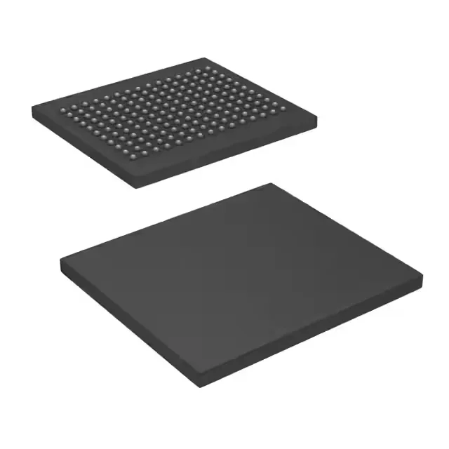
QDR II SRAM for high-bandwidth buffer applications
It clocks at 200 MHz on the parallel interface, delivering back-to-back read and write operations on separate data ports without bus-turnaround dead cycles — the defining advantage of QDR II over conventional synchronous SRAMs.
200 MHz clock — what it buys the system
At 200 MHz the QDR II architecture delivers a peak bandwidth of 1.6 GB/s on a 36-bit data bus (double-data-rate on both read and write ports). This matters for designs that must move large data blocks — packet buffers, look-up tables, or trace buffers — without stalling the processor or ASIC. The 1M x 36 organization gives a 36-bit word width that aligns naturally with 36-bit or 72-bit memory controllers, reducing the part count versus narrower x18 or x9 devices.
The 1.8 V supply rail needs local decoupling with low-ESR MLCCs placed within 2 mm of the BGA perimeter. Surface-mount only; no socket options exist for this package.
If your design can tolerate a different package or density, a QDR II+ or QDR IV family member from the same vendor may be a functional alternative, but pin-compatibility must be verified against the specific footprint.