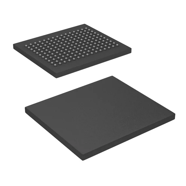
Cypress Semiconductor CY7C1414AV18-167BZI is a 36Mbit synchronous QDR II SRAM organized as 1M x 36, clocked at 167 MHz, operating from a 1.7V to 1.9V supply. The QDR II architecture provides separate read and write data ports, eliminating bus-turnaround dead cycles — a key feature for high-throughput networking, switch fabric, and telecom line-card designs. The official product status is Obsolete. Cypress has discontinued this part; there is no last-time-buy window remaining through the factory. No direct pin-compatible replacement is listed in the Cypress QDR II portfolio as a formal successor.
167 MHz clock and QDR II bus timing
The 167 MHz clock defines the maximum operating frequency for the synchronous interface. At this speed, the QDR II architecture delivers back-to-back read and write transactions without idle cycles on the data bus. The 1M x 36 organization gives a 36-bit-wide data word, suited for 32-bit or 36-bit datapath alignment in packet processing or lookup-table applications. The parallel memory interface requires careful PCB layout for the 165-ball BGA — the 15x17 mm footprint with a 1.0 mm ball pitch typical of this LBGA family. Supply decoupling on the 1.7V to 1.9V rail should follow the reference design recommendations for QDR II SRAM to maintain signal integrity at the rated clock edge.
The 165-LBGA (15x17 mm) is a standard BGA footprint; rework requires a preheat profile matching the package's moisture sensitivity level.