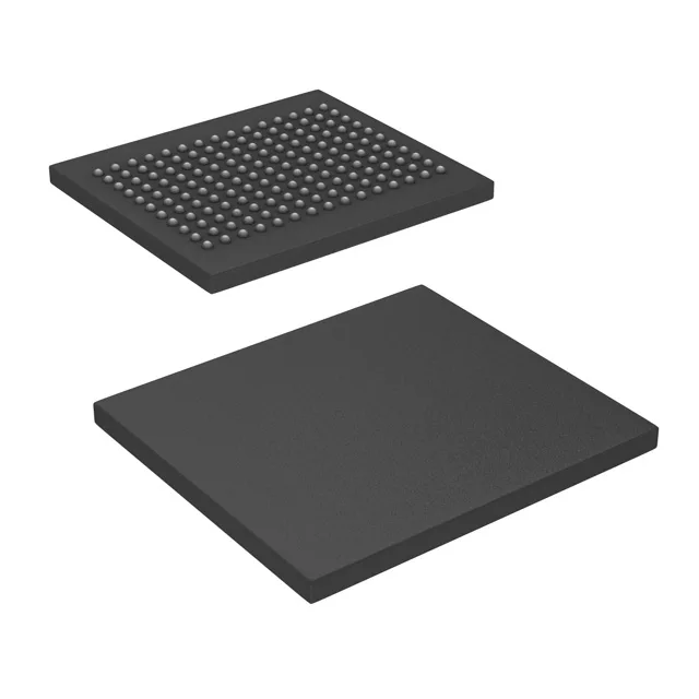
The CY7C1412AV18-250BZC comes in a 165-ball FBGA (15x17 mm body) — a fine-pitch BGA that demands a controlled solder-paste stencil and a reflow profile matched to the 0.8 mm ball pitch. The 165-FBGA footprint is standard for high-density synchronous SRAMs in this density class; the board layout must account for the 1.7–1.9 V core supply rail and the parallel bus routing to the memory controller.
Memory parametrics and throughput
At 250 MHz clock, the QDR II architecture delivers four data words per clock cycle — two on the rising edge and two on the falling edge of both the K and K# clocks — yielding a peak read/write bandwidth of 1 GB/s on the 18-bit data bus. The 2M x 18 organization (36 Mbit total) is suited for high-bandwidth, low-latency applications such as network packet buffers, line cards, and telecom switches where the SRAM's deterministic access time beats DRAM-based alternatives.
Temperature grade and supply range
The 1.7 V to 1.9 V supply range is the QDR II core voltage; the I/O voltage is separate and must be matched to the controller's interface level (typically 1.5 V or 1.8 V HSTL).