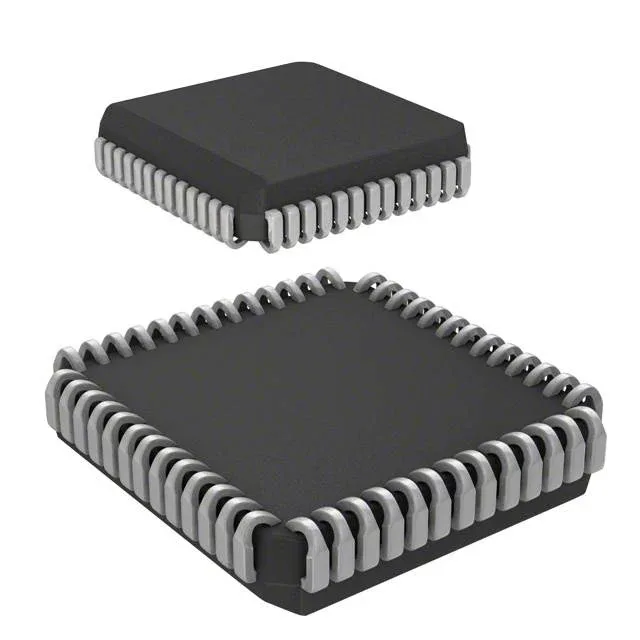
Dual-port SRAM for shared-memory designs
The Cypress CY7C141-25JC is an 8Kbit dual-port asynchronous SRAM organized as 1K x 8, delivering a 25 ns access time that allows two independent systems to read or write to the same memory array without bus contention logic.
A 25 ns access time means the SRAM can complete a read or write cycle in 25 ns from address valid, which translates to a 40 MHz maximum bus frequency in zero-wait-state designs. For a shared-memory link between two processors or an FPGA and a microcontroller, this timing leaves roughly 10–15 ns of margin after accounting for PCB trace delay and output hold times at 5V logic levels — enough for most through-hole or PLCC-based layouts without needing series termination.
52-PLCC J-lead — rework and footprint notes
The 52-PLCC (19.13 x 19.13 mm) J-lead package is a surface-mount part that can be hand-soldered or reflowed, but the J-lead geometry makes visual inspection of the solder joint tricky — you are trusting the fillet. The J-lead footprint is the same as a standard 52-PLCC socket, so a socketed prototype is an option if you are still debugging.
No direct pin-compatible replacement has been announced; the dual-port SRAM market has largely moved to higher-density synchronous parts or integrated dual-port blocks in FPGAs.