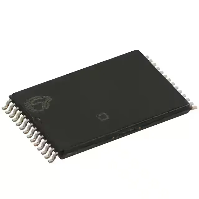
The CY7C1399BN-20ZXCT: Sourcing now runs through independent distribution, where available inventory is quoted against an RFQ.
20 ns access time — bus timing margin
The 20 ns access time is the key timing spec for this asynchronous SRAM. A host controller with a 25 ns or longer memory-cycle period can run this part with zero wait states; a faster bus may need to stretch the cycle or insert a wait state. The 20 ns figure is consistent with a 33 MHz to 40 MHz bus clock, assuming one-cycle access.
256Kbit density in 32K x 8 — buffer or scratchpad fit
Organised as 32K words of 8 bits each, this 256Kbit SRAM serves as a small-footprint data buffer, parameter store, or working scratchpad in embedded systems. The parallel interface ties directly to an MCU or FPGA local bus without serialisation overhead. For designs that need a byte-wide memory window in the 0x0000–0x7FFF address range, the 32K x 8 layout maps cleanly.
Rated supply range of 3V to 3.6V aligns with standard 3.3V logic families.
Package — 28-TSOP I, surface mount
Housed in a 28-TSOP I package, 11.80 mm body width, this is a standard thin small-outline package for memory devices. The surface-mount footprint suits automated assembly.