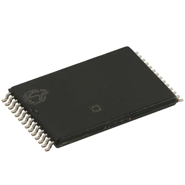
Infineon Technologies CY7C1399BN-15ZXC — Memory (DRAM / SRAM / Flash / EEPROM)

Infineon CY7C1399BN-15ZXC 256Kbit Async SRAM, 15ns

MPNCY7C1399BN-15ZXC
Obsolete

Infineon Technologies (Cypress) CY7C1399BN-15ZXC, 256Kbit asynchronous SRAM, 32K x 8 organization, 15 ns access time, 3.3 V supply, 28-TSSOP tray.

Sourced new & surplus through independent channelsAuthenticity-screened · ESD-safe packingListing updated Jul 2026

Specifications

CY7C1399BN-15ZXC specifications
ParameterValue
Memory typeVolatile
MountingSurface Mount
Voltage3V ~ 3.6V
Memory interfaceParallel
Operating temperature0°C ~ 70°C (TA)
PackageTray
TechnologySRAM - Asynchronous
Access time15 ns
Memory size256Kbit
Memory formatSRAM
Case28-TSSOP (0.465\", 11.80mm Width)
Memory organization32K x 8
Write cycle time - word, page15ns

Product details

Device identity and timing parametrics

The CY7C1399BN-15ZXC is a 256Kbit asynchronous SRAM from Infineon (formerly Cypress), organized as 32K x 8 bits. The 15 ns access time sets the window for the address-to-data valid path — the bus controller must sample the output within that window, and the 15 ns write cycle time (word, page) mirrors the same constraint on the write side. The commercial temperature grade (0°C to 70°C) limits it to indoor, controlled-environment boards — no extended or industrial range is specified.

This part is marked obsolete by the manufacturer. Sourcing is through independent distribution channels — quantities are confirmed per RFQ, and the buyer should verify date code and lot traceability at quote time.

Housed in a 28-TSSOP package (0.465" body width, 11.80 mm width) with a surface-mount footprint, the part is supplied in tray format. The supplier device package is designated 28-TSOP I — the standard thin small-outline package for this density class. The 0.65 mm pitch (typical for TSOP I) requires a controlled-impedance layout if the bus is shared with other fast SRAMs, but at 15 ns the trace-length matching is less critical than for synchronous memories.

Frequently asked questions

What does the 15 ns access time mean for my bus timing?

The 15 ns access time is the maximum delay from address valid to data valid on the output bus. The bus controller must sample the data within this window. The write cycle time is also 15 ns, so the same timing budget applies to the write strobe. At 3.3 V and 0°C to 70°C, derating the access time by 10-15% at the hot corner is prudent for marginal designs.