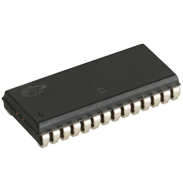
12 ns asynchronous SRAM — 28-SOJ footprint and board-fit
The CY7C1399B-12VC is a 256 Kbit asynchronous SRAM organized 32K x 8, with a 12 ns access time that sets the read-cycle floor for the memory bus — the processor or DMA controller must tolerate 12 ns from address valid to data valid on the parallel interface.
No pin-compatible replacement from the original manufacturer exists — a board spin to a different package or a different memory type is required for new production.
Parallel interface and bus timing
The memory interface is Parallel — address and data share the bus in a standard SRAM read/write cycle. The 12 ns access time and 12 ns write-cycle time mean the part supports bus speeds up to roughly 83 MHz in a zero-wait-state design, though the actual throughput depends on the controller's address-to-data setup and hold margins. As an asynchronous SRAM, it requires no refresh clock — the data persists as long as supply is within the 3 V–3.6 V range. This simplifies the glue logic compared to a synchronous SRAM or PSRAM, at the cost of higher standby current than a comparable DRAM.