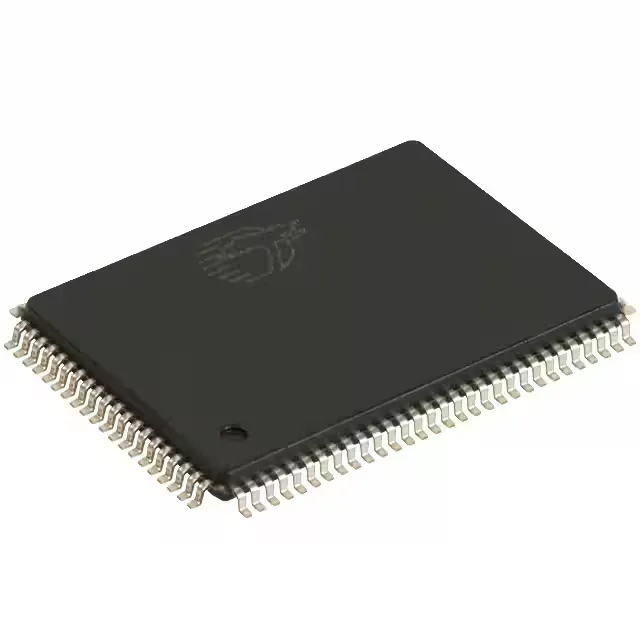
High-speed synchronous SRAM with NoBL architecture
200 MHz clock and 3 ns access — what they mean for timing closure
The 200 MHz clock frequency sets the maximum operating rate for the memory interface. At this speed, the 3 ns access time defines the window from clock edge to valid data on the bus. For a system architect, this means the FPGA or ASIC controller must budget for a 3 ns tCO plus board trace delay and still meet setup time on the receiving end. The 512K x 36 organization provides 18 Mbit of storage with a 36-bit wide data path, suitable for 32-bit plus parity or ECC applications.
The 100-TQFP (14x20 mm) package is a standard fine-pitch surface-mount footprint with 0.5 mm lead pitch.
Infineon has classified the CY7C1370D-200AXI as Obsolete. There is no pin-compatible direct replacement from Infineon's current SRAM portfolio; any substitution would require a board respin and revalidation of the memory controller timing.