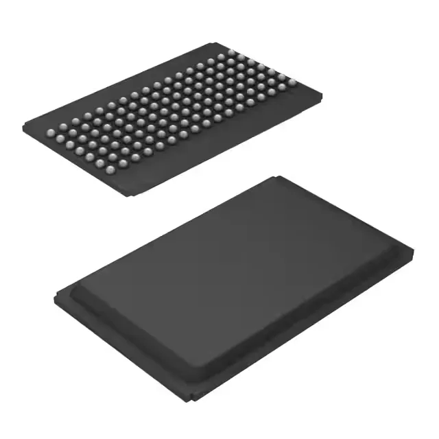
18 Mbit synchronous SRAM at 133 MHz — the 4.2 ns access time drives the bus budget
The Cypress CY7C1370B-133BGC is a 512K × 36 synchronous SRAM organized as 18 Mbit of fast static RAM, clocked at 133 MHz with a 4.2 ns access time from the clock edge. The 119-PBGA (14 × 22 mm) package places 119 balls on a 1.27 mm pitch — a surface-mount BGA that requires controlled reflow profiling and X-ray inspection post-assembly.
Cypress has discontinued production, so the only available inventory is new-old-stock or surplus held by independent distributors.
133 MHz clock and 4.2 ns access — timing closure for the memory controller
The 133 MHz clock rate sets the bus cycle at 7.5 ns, and the 4.2 ns access time from clock-to-data-valid gives the memory controller a 3.3 ns window for setup and hold before the next rising edge. That margin shrinks with PCB trace delay and on-die variation, so the layout engineer should keep the clock and data trace lengths matched within 0.5 inch and place the SRAM within 2 inches of the controller. The 3.135–3.6 V supply range means the part runs cleanly on a nominal 3.3 V rail with ±5 % tolerance — no extra regulator needed if the board already carries a 3.3 V plane.
512K × 36 organization — wide data path for networking and DSP buffers
The 36-bit word width maps directly to a 32-bit data bus plus 4 parity or ECC bits, common in network switch packet buffers and DSP coefficient storage. The synchronous interface eliminates the dead cycles of asynchronous SRAM — every clock edge can start a new read or write, sustaining the full 133 MHz throughput. The 0–70 °C commercial temperature grade limits this part to controlled indoor environments: office equipment, telecom central office, and instrument racks, not outdoor or under-hood deployment.