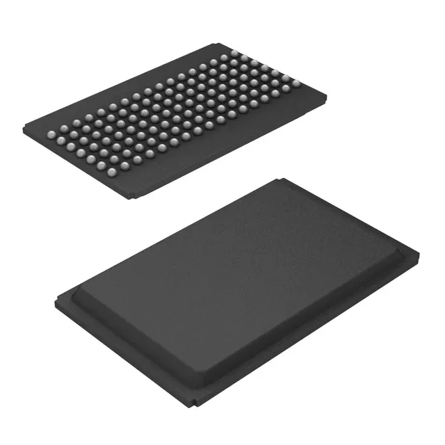
Infineon Technologies CY7C1361B-100BGC — Memory (DRAM / SRAM / Flash / EEPROM)

CY7C1361B-100BGC Infineon 9Mbit SRAM, 256Kx36, 100MHz

MPNCY7C1361B-100BGC
Obsolete

Infineon Technologies CY7C1361B-100BGC synchronous SRAM, 9Mbit, 256K x 36 organization, 100 MHz clock, 8.5 ns access time, 3.135V–3.6V supply, 119-PBGA (14x22), 0°C–70°C.

Sourced new & surplus through independent channelsAuthenticity-screened · ESD-safe packingListing updated Jul 2026

Specifications

CY7C1361B-100BGC specifications
ParameterValue
Memory typeVolatile
MountingSurface Mount
Voltage3.135V ~ 3.6V
Frequency100 MHz
Memory interfaceParallel
Operating temperature0°C ~ 70°C (TA)
PackageBag
TechnologySRAM - Synchronous, SDR
Access time8.5 ns
Memory size9Mbit
Memory formatSRAM
Case119-BGA
Memory organization256K x 36

Product details

256K x 36 synchronous SRAM — what the organization means for your bus

The CY7C1361B-100BGC is a 9Mbit synchronous SRAM organized as 256K words by 36 bits. The 36-bit word width matches a 32-bit data bus plus 4 parity or ECC bits — common in networking and telecom line-card buffers where the extra bits carry sideband or error-correction data without an external latch cycle. At a 100 MHz clock with an 8.5 ns access time, the part delivers one word per clock in burst mode — the pipelined synchronous interface hides the column-access latency behind the register stage.

119-PBGA footprint — board-fit constraints

Housed in a 119-ball PBGA measuring 14x22 mm, the package requires a 4+ layer PCB with buried vias for signal fan-out — the 0.80 mm ball pitch forces at least two signal layers to escape all 36 data lines plus address and control.

Frequently asked questions

What is the closest pin-compatible alternative to CY7C1361B-100BGC in this SRAM family?

The base product number CY7C1361 covers the 256K x 36 synchronous SRAM family; any replacement would need a board spin or a different package/pinout.