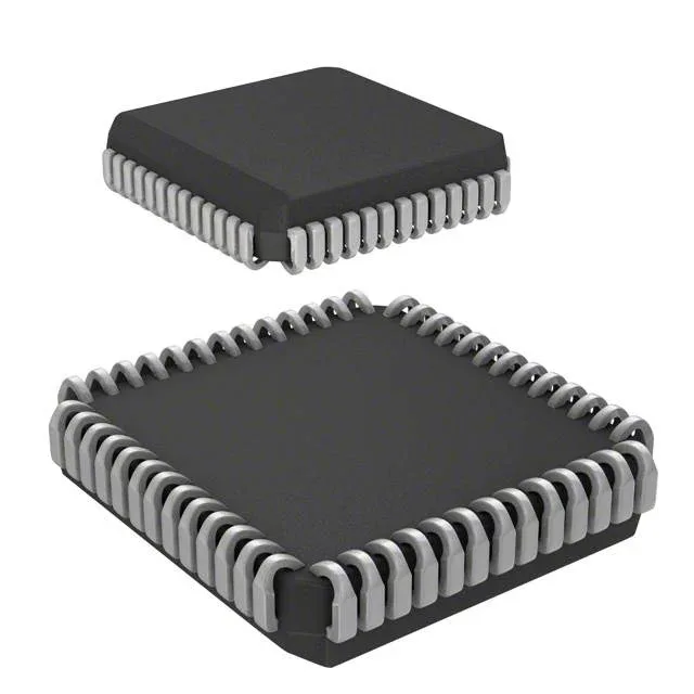
The Cypress CY7C136-55JXC is a 16Kbit asynchronous dual-port SRAM organized as 2K x 8 bits. Unlike a standard single-port SRAM, the dual-port architecture gives two independent buses simultaneous access to the same memory array, with on-chip arbitration logic to resolve simultaneous writes to the same address.
At 5 V operation, that timing is comfortable for 8-bit microcontrollers running at 10–12 MHz and for slow CPLD or FPGA state machines. If your host bus runs faster than about 18 MHz, the 55 ns window starts to eat into setup-and-hold margins, and you may need to insert wait states or move to a 25 ns or 15 ns dual-port SRAM.
Supply and temperature — commercial indoor only
No industrial or automotive variants of this exact order code exist; if your ambient exceeds 70°C, you need a different dual-port SRAM family rated for extended range.
52-PLCC footprint — legacy surface-mount
The 52-PLCC (J-lead) package measures 19.13 x 19.13 mm. It is a through-hole-compatible surface-mount form factor that was common in the 1990s and early 2000s. If your existing board uses a 52-PLCC socket or footprint, this part drops in. For a new design, the PLCC package is less common today than TQFP or BGA; factor in that the footprint is large relative to the 16Kbit density.
No direct pin-compatible replacement has been officially designated by the manufacturer. For a legacy BOM line that must be filled, the independent distribution channel is the only supply path. If you are designing a new shared-memory interface, consider a current-production dual-port SRAM from Cypress/Infineon or Renesas with a similar 2K x 8 organization and 5 V tolerance, but verify the PLCC footprint compatibility.