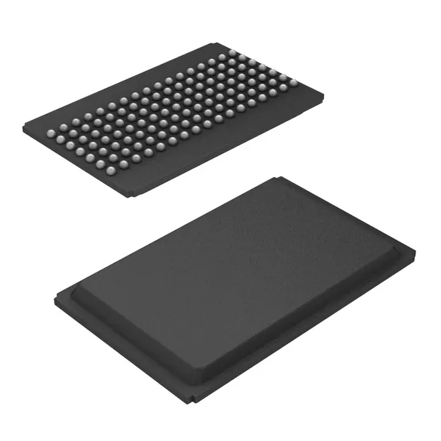
133 MHz synchronous SRAM with zero-bus-latency pipeline
The CY7C1355C-133BGXC is a 9Mbit synchronous SRAM organized as 256K x 36, clocked at 133 MHz with a 6.5 ns access time. It belongs to Infineon's NoBL (No Bus Latency) series, which eliminates the dead cycle between read and write operations — each clock edge can launch a new transaction regardless of the previous direction. The 36-bit data bus (32 data + 4 parity/byte-select) suits networking equipment that needs wide word access for packet buffer lookups or forwarding tables. The parallel interface keeps the bus simple — no serialization overhead, but the 119-ball BGA demands a controlled-impedance PCB layout with the supply decoupling close to the balls.
Core supply is 3.135 V to 3.6 V, nominally 3.3 V. The 0.465 V tolerance covers a 5% regulated rail plus transient droop — a 3.3 V buck converter with ±2% setpoint keeps the SRAM inside its window without a separate LDO. This limits the part to indoor, temperature-controlled environments — telecom central office, server room, or lab equipment.
Package and board-fit considerations
The 119-ball count means the outer rows carry address and control signals; the inner array is mostly Vdd and Vss. A four-layer board with a solid ground plane under the BGA is the minimum for signal integrity at 133 MHz.
Obsolete — sourcing through surplus channels
Each lot is sourced and verified against the BOM quantity at RFQ — no stock-holding claim is made. The 119-BGA package and 3.3 V supply mean a board spin is required to use any alternative SRAM with a different footprint or voltage.