Synchronous SRAM for wide-bus, high-throughput designs
The 36-bit word width suits applications that move wide data words per cycle — network switch buffers, telecom line-card packet memories, or DSP coefficient storage where bus turnaround overhead must be eliminated.
NoBL architecture — what the 133 MHz clock and 6.5 ns access mean for the bus
The NoBL pipeline eliminates the dead cycle between read and write transitions that conventional synchronous SRAMs require. At 133 MHz, each clock cycle is 7.5 ns; the 6.5 ns access time means data appears on the outputs within one clock edge of the address being latched, leaving roughly 1 ns of setup margin before the next rising edge. For a system architect, this translates to sustained back-to-back throughput at the full clock rate — no bubble cycles to budget for. The 36-bit data bus, combined with the 256K address depth, gives a total memory footprint of 9 Mbit, which is sized for moderate-depth lookup tables or FIFO emulation in FPGA-attached memory.
Cypress (now part of Infineon) no longer manufactures this specific variant.
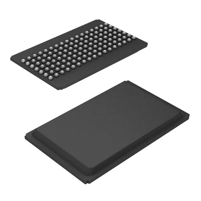
Package and footprint — 119-ball PBGA (14x22 mm)
The ball pitch is 1.27 mm, which is a standard BGA pitch that routes through a four-layer PCB without microvias. The package is surface-mount only. The supplier device package code is 119-PBGA (14x22). The shipping medium is Tray, not tape-and-reel, so pick-and-place lines will need a tray feeder or a bulk-to-tape conversion step.