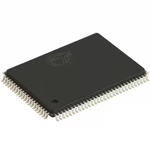
Package and board integration — 100-TQFP, 0.5 mm pitch
The CY7C1354C-166AXI: The 100-TQFP (14x20 mm) footprint uses a 0.5 mm pitch peripheral lead array — no hidden balls, so visual inspection and rework are straightforward. The exposed pad on the bottom of the package is the primary thermal path; a thermal via array under the pad keeps the junction below 85°C in still-air environments.
166 MHz synchronous burst and 3.5 ns access — what it means for timing
At 166 MHz the clock period is 6.0 ns. The 3.5 ns access time from clock edge to data valid leaves 2.5 ns of setup margin before the next clock edge — enough for a moderate PCB trace delay but tight for backplane routing. The 256K x 36 organization delivers a 36-bit word every clock cycle, so a 64-bit data bus needs two devices in parallel with the address and control lines shared.
Supply and temperature — single 3.3 V rail, industrial range
Runs from a single 3.135 V to 3.6 V supply, matching the 3.3 V I/O voltage of most FPGAs and ASICs without a separate VDDQ rail. The -40°C to +85°C industrial temperature grade covers factory-floor automation, outdoor telecom cabinets, and unventilated enclosures.