What the 133 MHz clock and 4 ns access mean on the bench
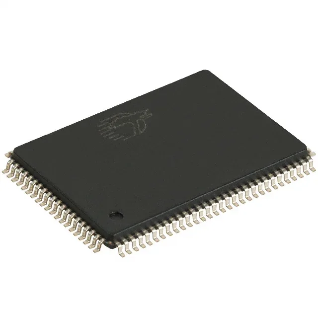
The CY7C1339G-133AXI is a 4Mbit synchronous SDR SRAM organized as 128K x 32 bits, clocked at 133 MHz with a 4 ns access time from the clock edge. That 4 ns window is the time from clock rising edge to data valid on the bus — at 133 MHz the cycle time is 7.5 ns, so the part leaves 3.5 ns for the downstream logic setup before the next clock. If you are debugging a board that reads back stale data, check whether the FPGA or ASIC's input hold time eats into that margin.
Obsolete — what that means for your BOM line
This part is marked obsolete by Infineon. No official successor or pin-compatible replacement is listed on the record. For a repair bench or a legacy production run, the only channel is independent surplus inventory — no factory last-time-buy window remains open.
Supply rails and temperature grade
Runs on a single 3.15 V to 3.6 V rail — no separate Vddq or Vtt.