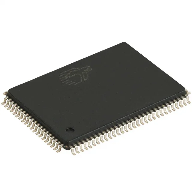
What this synchronous SRAM does on the board
The Cypress CY7C1328G-133AXI is a 4.5 Mbit synchronous SRAM organized as 256K x 18 bits, clocked at 133 MHz with a 4 ns access time. This part is typically used as a high-speed buffer or cache in networking switches, telecom line cards, and industrial controllers where deterministic read/write latency at clock frequency is critical.
133 MHz and 4 ns access — what that means for timing closure
The 133 MHz clock rate and 4 ns access time let this SRAM keep pace with high-throughput ASICs and FPGAs without inserting wait states. For a system architect, that 4 ns access window sets the setup-and-hold budget on the data bus; if your controller's output valid window is tighter than 4 ns, you'll need to account for board trace delay and clock skew. At 133 MHz, the synchronous pipeline registers the address and control signals on the rising edge, so the memory controller must meet the setup time relative to that edge — something to verify in your timing analysis.
No further factory orders are accepted, and no last-time-buy window remains open. If this part is on your BOM, you are now in the surplus and independent-distribution channel. There is no official Cypress successor listed for this exact order code, so any replacement will require a pin-compatible or functionally equivalent alternative from a different vendor.