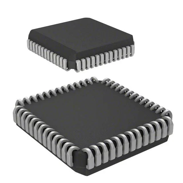
8Kbit dual-port SRAM — 55 ns access time
The CY7C131-55JXCT: Organized as 1K x 8, this dual-port asynchronous SRAM allows simultaneous read/write access from two independent ports — useful for shared-memory buffering between processors or between a processor and an FPGA. 55 ns access time and 55 ns write cycle time set the bus timing floor. In a shared-memory arbitration scheme, the port-to-port handshake must accommodate this delay to avoid data contention. Operates from a single 4.5V to 5.5V supply — a legacy 5V rail, common in industrial and telecom backplanes where the CY7C131 series was originally designed in.
52-PLCC package — board-fit considerations
Supplied in a 52-lead PLCC (J-lead) package, supplier device package 52-PLCC (19.13x19.13 mm). The J-lead footprint is surface-mount but requires a PLCC socket or a reflow profile compatible with the lead pitch. Tape & Reel packaging indicates it was originally intended for automated pick-and-place assembly. For prototype or low-volume builds, verify the PLCC socket availability against the 52-position JEDEC footprint. Commercial temperature range (0°C to 70°C) — suitable for indoor equipment, not extended or industrial thermal environments.