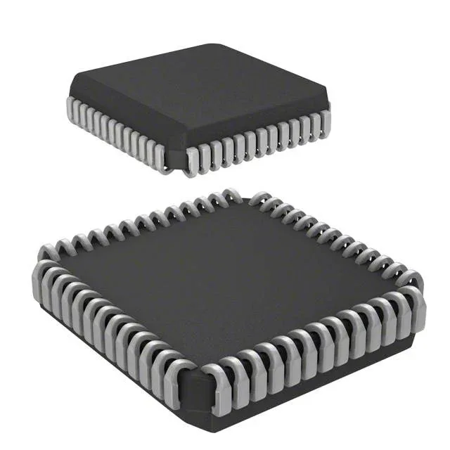
25 ns dual-port SRAM for shared-memory handshaking
The Cypress CY7C131-25JXCT is an 8Kbit dual-port asynchronous SRAM organized as 1K x 8, with a 25 ns access time that sets the bus timing budget for the system. This part lives in the 52-PLCC J-lead package, a footprint common on legacy telecom line cards, industrial controller backplanes, and multiprocessor shared-memory designs where two independent buses need collision-free access to a single buffer.
If your design can tolerate a footprint or voltage change, a newer dual-port SRAM family (such as the CY7C028 or CY7C144 series in a different package) may be a candidate — but that requires a board spin and timing revalidation.
What the 25 ns access time means for the bus
In a dual-port configuration, both ports can initiate reads or writes independently, and the arbitration logic handles simultaneous access to the same memory location. The 25 ns window sets the minimum cycle time for the bus master — a 40 MHz bus clock (25 ns period) just meets the spec, but you lose margin for address setup, hold, and propagation delay through buffers. For a 20 MHz bus (50 ns period), the 25 ns access gives comfortable timing headroom.
8Kbit in a 52-lead PLCC — what it tells you
An 8Kbit memory in a 52-pin package is a strong hint that the die area is dominated by the dual-port arbitration logic and the I/O ring, not the memory array. The 1K x 8 organization means each port sees a flat 1K address space, one byte wide — useful for a mailbox register, a small FIFO, or a parameter block shared between two processors. The 52-PLCC (19.13 mm x 19.13 mm) is a J-lead surface-mount package that can be hand-soldered with care, though the J-lead form makes visual inspection of the solder joint harder than a gull-wing. The Tape & Reel suffix (CT) indicates it ships on a reel, not tube or tray.