Cypress no longer produces this part, and no factory last-time-buy window remains open.
15 ns access time — the arbitration margin
The CY7C131-15JXC is an 8Kbit (1K x 8) dual-port asynchronous SRAM from Cypress. In a dual-port arbitration scenario — where two independent bus masters (e.g., a DSP and an FPGA) share the same memory array — the 15 ns window sets the bus-turnaround margin. At a 33 MHz bus clock (30 ns period), a single access fits comfortably within one cycle; at 66 MHz (15 ns period), the access time equals the clock period, leaving zero margin for address hold or data setup. Designs running above 33 MHz should budget for one wait state or consider a faster dual-port SRAM.
Dual-port architecture — no external arbiter needed
As a dual-port SRAM, the CY7C131 integrates two independent address, data, and control ports that access a common 1K x 8 memory array. On-chip arbitration logic handles simultaneous access to the same address — the part asserts a BUSY flag on one port while the other completes the cycle.
52-PLCC footprint — legacy package, socket-friendly
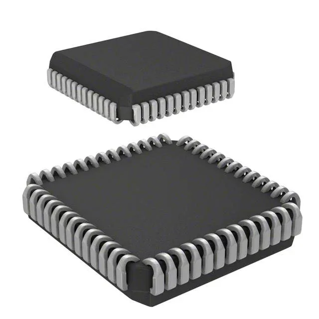
The CY7C131-15JXC comes in a 52-lead PLCC (J-lead) package, supplier device package 52-PLCC (19.13x19.13 mm). The J-lead form factor is through-hole compatible with a PLCC socket, making it suitable for prototyping, rework, and systems where field replacement is expected. The surface-mount PLCC footprint requires a standard 52-pin JEDEC land pattern. The shipping medium is Tube.
Supply and temperature — 5 V nominal, commercial range
This limits deployment to temperature-controlled indoor environments — office equipment, telecom racks, test instrumentation — and excludes automotive under-hood or industrial outdoor applications without active thermal management.