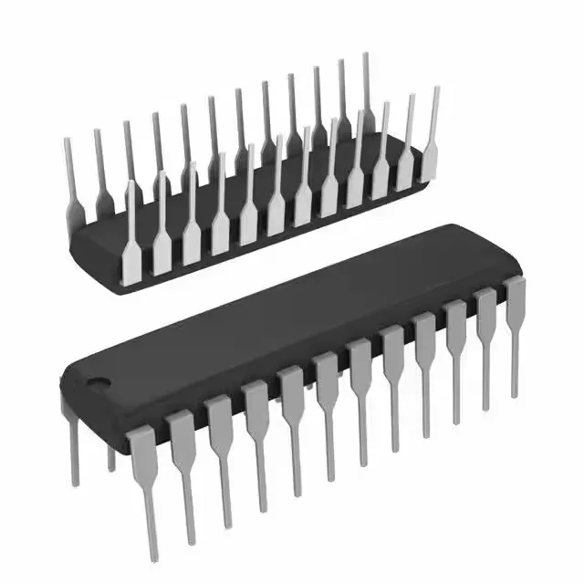
Legacy 5V asynchronous SRAM in a through-hole DIP
Housed in a 24-pin plastic DIP (PDIP-24) with 0.300-inch body width, it is a through-hole part intended for socketed or wave-soldered boards. This is a legacy 5V logic-level memory, not compatible with 3.3V or lower-voltage buses without external level shifters.
45 ns access time — bus timing budget
For a legacy 8-bit microcontroller or ASIC running at 10–20 MHz, this allows one or two wait states depending on the memory controller's setup. This is a relatively slow part by modern standards — a 10 ns SRAM like the CY7C1049G-10VXI runs four times faster — but for 1980s/1990s-era bus architectures, 45 ns was a standard speed grade.
16 Kbit density — small scratchpad or cache
At 16 Kbit (2,048 bytes), this SRAM is sized for small data buffers, parameter storage, or a secondary cache in embedded controllers. It is not a main memory device; its role is to offload frequently accessed variables from a slow EPROM or to serve as a temporary FIFO in a data acquisition path. The 2K x 8 organization maps cleanly to an 8-bit data bus without byte-lane steering.
RoHS non-compliant — lead-bearing terminations
It is not exempt under the standard RoHS exemptions for lead in solder for servers/storage or for lead in ceramic packages. New designs targeting RoHS compliance (e.g., EU markets, consumer goods) cannot use this part unless an exemption applies. For legacy repair, MRO, or military/avionics BOMs that specify SnPb solder, this is the correct finish.
Active lifecycle — no EOL risk
Package and mounting — through-hole only
The 24-pin PDIP package (0.300-inch row spacing, 7.62 mm) is a through-hole format. It is designed for socketed insertion or wave soldering, not for reflow. Board layout requires 0.100-inch (2.54 mm) pitch holes. The shipping medium is Tube, not tape-and-reel.