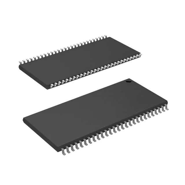
The Infineon CY7C1069AV33-12ZXCT is a 16 Mbit asynchronous SRAM organized as 2M x 8, with a 12 ns access time that sets the timing budget for the processor-to-memory interface. The 12 ns write cycle time matches the read access, so back-to-back reads and writes run at the same speed without dead cycles.
2M x 8 organization — byte-wide memory for 8-bit or muxed buses
Organized as 2M words of 8 bits each, this SRAM connects directly to an 8-bit data bus. In a 16-bit or 32-bit system, you need two or four devices with the address lines shared and the chip selects decoded — or external byte-lane muxing. The parallel interface is straightforward: address, data, chip enable, output enable, and write enable. No clock, no burst logic, no refresh cycles — the asynchronous nature simplifies timing closure but means every access takes the full 12 ns cycle.
Infineon lists the CY7C1069AV33-12ZXCT as obsolete. For BOM lines that still require this part, procurement must turn to independent distribution and surplus channels. The 54-TSOP II footprint is shared across many asynchronous SRAMs in the 16 Mbit density range, but pin compatibility with any specific alternate needs to be verified against the target system's timing and supply requirements.
54-TSOP II — footprint and rework
Housed in a 54-TSOP II (0.400 inch body width, 10.16 mm), this is a fine-pitch surface-mount package. The Tape & Reel shipping form indicates it was intended for high-volume pick-and-place. For rework, the typical hot-air profile for TSOP packages applies — preheat the board to 125 °C, then focus the nozzle on the package body until the solder reflows. Inspect for bridges under magnification; the 0.5 mm lead pitch leaves little room for error.