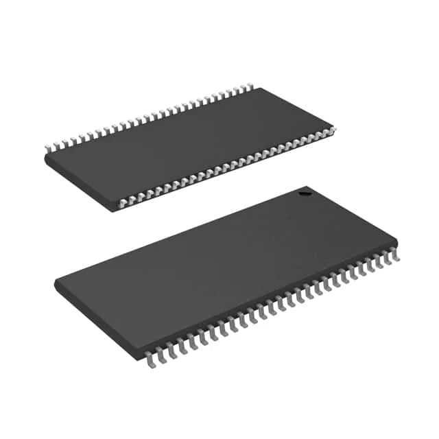
16 Mbit async SRAM for legacy bus interfaces
This is a volatile memory, meaning data is retained only while power is applied.
10 ns access time — timing margin for the memory controller
The 10 ns access time and 10 ns write cycle time set the bus timing budget. For a controller running at 100 MHz, this gives a 10 ns window to latch data after the address is stable — enough margin for a single-cycle read without wait states, provided the board trace lengths are kept under about 60 mm (roughly 1 ns per 150 mm FR4 propagation). If the controller is faster than 100 MHz, you will need to insert wait states or look at a synchronous SRAM.
Infineon lists the CY7C1069AV33-10ZXIT as Obsolete. No direct factory replacement is published. For new designs, consider a pin-compatible asynchronous SRAM from the same 54-TSOP II footprint family, such as the ISSI IS61WV20488BLL.
54-TSOP II — rework and layout considerations
The 54-TSOP II package (0.400 inch body width, 10.16 mm) has a 0.5 mm pitch. It is a fine-pitch gull-wing lead form that reflows reliably with a standard profile.