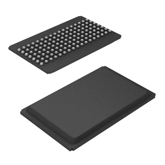
16 Mbit asynchronous SRAM in a 32-bit bus width
The Infineon CY7C1062GE30-10BGXI is a 16 Mbit asynchronous SRAM organized as 512K x 32 bits. It delivers a 10 ns access time across a 2.2 V to 3.6 V supply range, operating from -40°C to 85°C. The parallel interface and 119-ball BGA package (14x22 mm body) target high-speed cache, networking buffers, and industrial control applications where deterministic read/write latency matters and a 32-bit data bus matches the processor or FPGA memory controller width.
Access time is 10 ns for read and write cycles. Write cycle time is also 10 ns in word and page mode.
512K x 32 vs x16 siblings — which bus width fits
The 512K x 32 organization is the key differentiator from the x16 variants in the same family. The CY7C1061G30-10BVXI (1M x 16) offers the same 16 Mbit density and 10 ns access but in a 16-bit bus — that halves the pin count on the memory interface but doubles the address space per chip select. The CY7C1062GE30-10BGXI is the part to pick when the processor or FPGA memory controller expects a 32-bit word width and you want a single-chip solution rather than two x16 devices in parallel. The 119-ball BGA footprint is larger than the 48-ball TSOP on the x16 parts, so board area and routing density factor into the choice.