10 ns asynchronous SRAM — timing and density for the BOM line
The CY7C1062AV33-10BGCT is a 16 Mbit asynchronous SRAM organized as 512K words by 32 bits, with a 10 ns access time from address valid to data valid on the bus. Operating from a single 3V to 3.6V supply, it presents a parallel memory interface that connects directly to a 32-bit data bus without the latency of a synchronous clock — the read cycle completes within the access-time window, which at 10 ns sets a 100 MHz theoretical ceiling on the address-to-data throughput. The commercial temperature range (0°C to 70°C) limits this part to equipment that stays inside a conditioned environment — a telecom line card in a climate-controlled central office fits; an outdoor base-station controller with passive cooling does not.
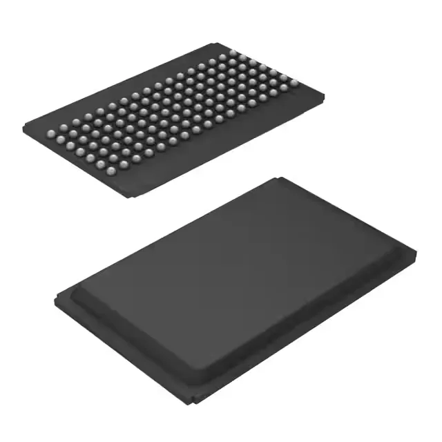
For a BOM line that already carries this footprint and timing, the supply path runs through independent distribution — quantities are lot-specific and confirmed at RFQ, with no factory lead time to quote. The 119-ball PBGA (14x22 mm body) is a fixed footprint; any pin-compatible drop-in would require the same ball map and supply voltage range, which no current-production part from Infineon or a second-source vendor is listed as matching.
Package and supply integration
The Tape & Reel packaging means the reel quantity and the MSL level (not listed here) govern the bake profile before reflow; a reel that has exceeded its floor life requires a bake cycle that delays the assembly run. The 3V–3.6V supply rail must match the memory controller's I/O voltage — a controller running at 1.8V or 2.5V will need a level translator on the address and data bus, adding propagation delay that cuts into the 10 ns access-time budget.