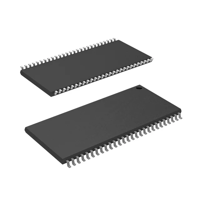
10 ns access time — timing margin for the bus
The spec record flags this part with an EOL-hot lifecycle stage, while the lifecycle field lists it as Active. This discrepancy suggests a transition phase.
This is a standard asynchronous SRAM — no clock, no burst mode, no DDR interface. The control pins are chip enable, output enable, and write enable. The 10 ns write cycle time means a single 10 ns pulse on write enable latches the data. For applications that need back-to-back reads and writes without bus-turnaround penalties, this part delivers because the asynchronous interface has no dead cycles between read and write transitions.