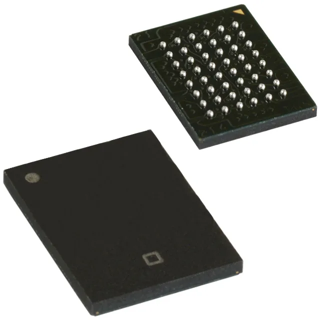
16 Mbit asynchronous SRAM with 10 ns access — bus timing fit
10 ns access time sets bus timing margin for interfacing to a processor or FPGA memory controller. 1M x 16 organization matches a 16-bit data bus without byte-lane muxing, saving glue logic.
Where it fits — industrial and embedded applications
Asynchronous SRAM with a 10 ns cycle time is a common choice for cache tag RAM, packet buffers in network switches, and real-time control data storage in factory automation and motor drives.
The CY7C1061GE30-10BV1XIT is listed with an EOL hot lifecycle status, meaning the manufacturer has announced end-of-life and a last-time-buy window is active or imminent. Procurement should plan for a bridge buy or identify a drop-in replacement before the LTB closes.