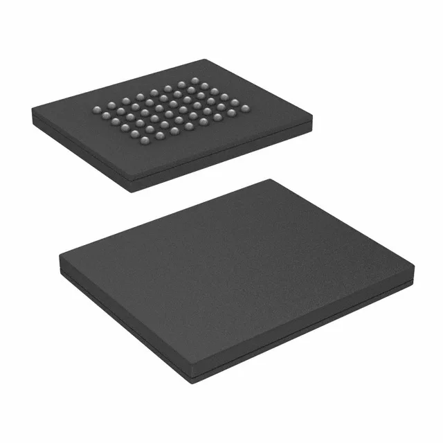
The CY7C1061DV33-10BVJXIT: This class of fast, wide-bus SRAM is typically used as a data buffer, cache tag store, or frame buffer in networking equipment, industrial controllers, test instrumentation, and telecom line cards where deterministic access latency matters more than density.
10 ns access time — the bus timing decision
The 10 ns access time and 10 ns write cycle time keep the bus symmetric for 16-bit wide reads and writes.
That means new-manufacture units are no longer available through the factory channel. If this SRAM is on your BOM, securing stock for production runs or spares requires a qualified distributor who can source from the open market and verify authenticity.
The 48-VFBGA (8x9.5 mm) is a fine-pitch ball-grid array. This is not a hand-solderable package — it needs a reflow oven or hot-air station with a profile tuned for the 0.5 mm or 0.65 mm ball pitch typical of VFBGA. The small body and low ball count make it less thermally challenging than a large BGA, but the balls are hidden under the package, so X-ray inspection is the only way to confirm solder joint integrity after reflow. Orientation is marked by the usual corner ball or silkscreen dot; confirm pin 1 location on the board layout before placing the part. If your assembly line is not set up for BGA rework, this package adds cost and risk versus a TSOP or SOJ alternative.