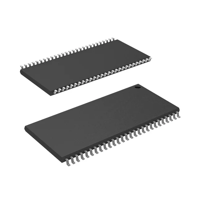
The CY7C1061AV33-12ZXI is a 16Mbit parallel SRAM organized as 1M x 16, with a 12 ns access time that sets the read-cycle floor for the memory bus — the controller must sample data within this window, and any bus loading beyond the datasheet's output drive spec stretches the effective access beyond the rated 12 ns.
Infineon lists the CY7C1061AV33-12ZXI as Obsolete.
Supplied in a Tray, surface-mount 54-TSOP II (0.400-inch, 10.16 mm width). The 0.50 mm pin pitch demands a controlled-impedance layout for the parallel address/data bus — trace-length matching within 500 mils keeps the 12 ns access window from being consumed by skew. Write cycle time is also 12 ns for word and page modes — the write strobe must be asserted for at least this duration. The asynchronous interface needs no clock, simplifying the FPGA or ASIC glue logic, but the setup/hold times relative to the address bus are tighter than a synchronous SRAM of the same density.