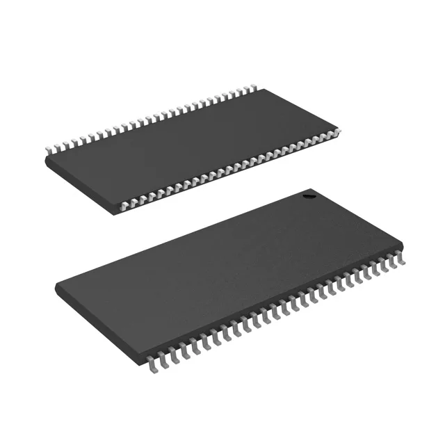
It is a volatile memory in a 54-TSOP II package, intended for parallel-interface cache, buffer, or scratchpad duty in networking, telecom, or embedded systems where deterministic read/write latency matters. The 10 ns access means the part can complete a random read or write in a single 100 MHz bus cycle without wait states, assuming the controller meets the setup/hold window. The 1M x 16 organization is a standard word-width for 16-bit data buses, giving a direct match to many PowerPC, x86, or ARM memory controllers without external byte-lane logic.
The 54-TSOP II footprint and 10 ns speed grade are common enough that a pin-compatible drop-in from another vendor (e.g., ISSI, Alliance Memory) may exist, but no cross-reference is documented here. If you are qualifying a replacement, the key parameters to match are the 1M x 16 organization, 10 ns access, 3.3 V supply, and the JEDEC-standard 54-TSOP II pinout.
Temperature grade and environment — indoor only
It belongs in office equipment, lab instruments, or indoor telecom racks — not in a motor drive, engine bay, or outdoor base station without active cooling or a temperature-grade upgrade. The 3.3 V supply (3V to 3.6V) is the standard for late-90s/early-2000s SRAMs; if your system runs at 3.0 V nominal, confirm margin at the low end of the range.
Package and mounting — 54-TSOP II on the board
Housed in a 54-TSOP II (0.400" body width, 10.16 mm), surface-mount package. No thermal pad or exposed paddle; standard reflow profile for a thin small-outline package applies.