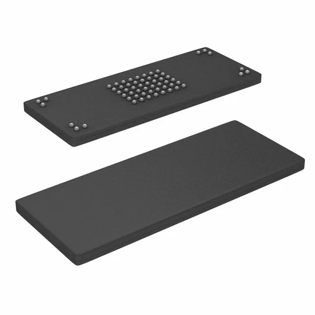
The Infineon CY7C1061AV33-10BAXI is a 16Mbit asynchronous SRAM organized 1M x 16, in a 60-TFBGA package. This is a volatile memory — data is lost at power-down. The asynchronous interface means no clock to route: address and control signals latch on the falling edge of chip enable or write enable, making it a straightforward drop-in for legacy bus designs or FPGA block RAM expansion.
Infineon (formerly Cypress) has ended production — no last-time-buy window remains open through the factory channel.
60-FBGA footprint — layout and rework notes
The PCB layout engineer needs a four-layer minimum with microvia capability or at least via-in-pad for the inner balls. Decoupling calls for one 100 nF ceramic per supply ball pair, placed within 2 mm of the ball, plus a 4.7 µF bulk cap on the 3.3V plane. The 10 ns write cycle time (word, page) matches the read access — no asymmetry penalty when the bus alternates read/write cycles at full speed. The write enable timing relative to chip enable is the critical path for the firmware bring-up engineer to verify in the first memory test routine.