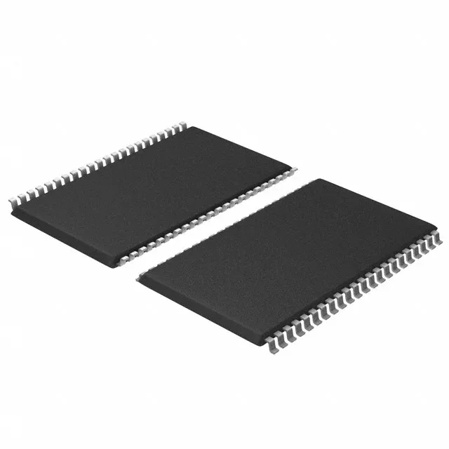
Infineon Technologies CY7C1051DV33-10ZSXIT — Memory (DRAM / SRAM / Flash / EEPROM)

Infineon CY7C1051DV33-10ZSXIT 8Mbit Async SRAM, 10 ns

MPNCY7C1051DV33-10ZSXIT
Obsolete

Infineon CY7C1051DV33-10ZSXIT, 8Mbit asynchronous SRAM, 512K x 16 organization, 10 ns access time, 3V to 3.6V supply, -40°C to 85°C industrial temperature, 44-TSOP II package, Tape & Reel.

$11.4700Ref. price · indicative, final on quote
Independent supplier — new & surplus stockAuthenticity-screened · ESD-safe packingListing updated Jul 2026

Specifications

CY7C1051DV33-10ZSXIT specifications
ParameterValue
Memory typeVolatile
MountingSurface Mount
Supply voltage3V ~ 3.6V
Memory interfaceParallel
Operating temperature-40°C ~ 85°C (TA)
PackageTape & Reel (TR)
TechnologySRAM - Asynchronous
Access time10 ns
Memory size8Mbit
Memory formatSRAM
Case44-TSOP (0.400\", 10.16mm Width)
Memory organization512K x 16
Write cycle time - word, page10ns

Product details

The Infineon CY7C1051DV33-10ZSXIT is an 8Mbit asynchronous SRAM organized as 512K x 16 bits, with a 10 ns access time and a parallel interface. It operates from a 3V to 3.6V supply, making it a direct fit for 3.3V bus systems in networking gear, telecom line cards, industrial controllers, and test equipment that need fast scratchpad or cache memory without refresh overhead.

The 10 ns access time and 10 ns write cycle time allow read or write operations at that speed.

Industrial temperature grade

Frequently asked questions

What is the replacement for CY7C1051DV33-10ZSXIT?

No official replacement part number is listed in the lifecycle record. For a pin-compatible alternative, you would need to cross-reference other 8Mbit asynchronous SRAMs in the 44-TSOP II footprint with a 10 ns access time and 3.3V supply — but no direct Infineon successor is documented.

Is CY7C1051DV33-10ZSXIT compatible with 3.3V systems?

Yes, the supply range is 3V to 3.6V, so it operates directly on a 3.3V rail without a level shifter. The parallel interface is 3.3V logic-compatible.

What is the pinout of CY7C1051DV33-10ZSXIT?

The part is in a 44-TSOP II package (0.400" body width, 10.16 mm). The standard asynchronous SRAM pinout applies: address lines A0-A18, data lines DQ0-DQ15, chip enable, output enable, write enable, and power/ground. Pin 1 is marked on the package.