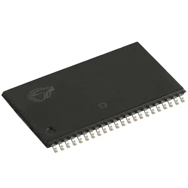
Infineon Technologies CY7C1049CV33-15ZSXE — Memory (DRAM / SRAM / Flash / EEPROM)

Infineon CY7C1049CV33-15ZSXE SRAM, 4Mbit, 15ns, 44-TSOP II

MPNCY7C1049CV33-15ZSXE
Obsolete

Infineon CY7C1049CV33-15ZSXE, asynchronous SRAM, 4Mbit (512K x 8), 15 ns access time, parallel interface, 3V to 3.6V supply, -40°C to 125°C, 44-TSOP II, Tube.

Sourced new & surplus through independent channelsAuthenticity-screened · ESD-safe packingListing updated Jul 2026

Specifications

CY7C1049CV33-15ZSXE specifications
ParameterValue
Memory typeVolatile
MountingSurface Mount
Voltage3V ~ 3.6V
Memory interfaceParallel
Operating temperature-40°C~125°C(TA)
PackageTube
TechnologySRAM - Asynchronous
Access time15 ns
Memory size4Mbit
Memory formatSRAM
Case44-TSOP (0.400\", 10.16mm Width)
Memory organization512K x 8
Write cycle time - word, page15ns

Product details

What this SRAM is and where it fits

The Infineon CY7C1049CV33-15ZSXE is a 4 Mbit asynchronous SRAM organized as 512 K x 8 bits, with a 15 ns access time and a parallel interface. It operates from a 3 V to 3.6 V supply and is rated for -40°C to 125°C.

15 ns access time — what it means for the bus

The 15 ns access time sets the window for the memory controller to latch valid data after asserting the address. The write cycle time matches at 15 ns.

Obsolete — sourcing reality

Infineon lists the CY7C1049CV33-15ZSXE as obsolete. No official successor is published in the lifecycle record. For a BOM line that needs this exact footprint and timing, the supply path is through surplus and independent distribution. We source and quote this part to order against an RFQ; availability and current pricing are confirmed at quote time.

Frequently asked questions

What is the replacement for CY7C1049CV33-15ZSXE?

No official replacement is listed in the lifecycle record. For a pin-compatible drop-in, you would need to evaluate other 512K x 8 asynchronous SRAMs in the 44-TSOP II package with a 15 ns access time and 3.3 V supply — but no direct successor is published by Infineon.

What is the CY7C1049CV33-15ZSXE pinout?

The CY7C1049CV33-15ZSXE uses the standard 44-TSOP II pinout for a 512K x 8 asynchronous SRAM. The datasheet PDF provides the full pin assignment and functional diagram.

CY7C1049CV33-15ZSXE vs CY7C1049CV33-12ZSXE?

The CY7C1049CV33-12ZSXE is the faster variant with a 12 ns access time versus 15 ns on this part. Both share the same 4 Mbit density, 44-TSOP II package, and 3.3 V supply. The 12 ns part offers tighter timing margin for higher-speed controllers but is also obsolete.