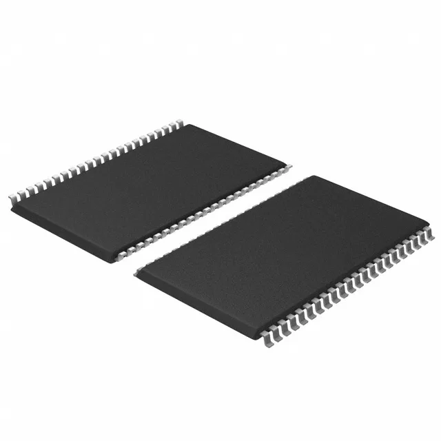
10 ns asynchronous SRAM for cache and buffer duty
The CY7C1041GN30-10ZSXI is a 4 Mbit asynchronous SRAM from Infineon Technologies, organized as 256K words by 16 bits. The 10 ns access time sets the read-cycle ceiling — at this speed the part serves as a look-up table, packet buffer, or CPU cache in systems where a clocked SRAM interface adds unnecessary complexity.
Package and board-fit constraints
Housed in a 44-TSOP II package (0.400-inch body width, 10.16 mm), the part mounts on the PCB surface with a standard JEDEC footprint. The 44-pin TSOP II layout is shared across multiple SRAM densities in the CY7C1041 family, so a single board layout can accept 4 Mbit, 8 Mbit, or 16 Mbit variants with the same pinout — useful for a BOM that scales memory across product tiers. Supplied in Tray packaging, the device is suited for pick-and-place assembly in medium-to-high volume production. The parallel memory interface requires 16 data lines plus address and control signals — the PCB routing must match the 10 ns timing budget, particularly the address-to-output propagation delay through the trace length.
Active lifecycle and compliance posture
As a volatile memory device, it requires a continuous power supply to retain data; no battery-backup or non-volatile storage is integrated.