4 Mbit async SRAM with 10 ns access — the bus-timing anchor
The CY7C1041G-10ZSXI: The parallel interface and 16-bit data width make it a direct fit for legacy 5V DSPs, CPLDs, and ASICs that need fast scratchpad memory or data buffering without the overhead of SDRAM controllers. Typical applications include industrial motor drives, telecom line cards, test equipment, and any system where deterministic read/write latency matters more than density.
For a 50 MHz bus (20 ns period), that leaves 10 ns of setup/hold margin before the next clock edge — enough to avoid wait states in most glue-logic designs. If your host bus runs faster than 66 MHz, you will need to budget the access time against the controller's output-hold spec; at 50 MHz and below this part keeps the timing clean.
5V supply — legacy system fit
No level shifters are needed on the address/data bus when connecting to a 5V host. If your new design has migrated to 3.3V, the sibling CY7C1041GE30-10ZSXI runs from a 3.0V supply and is otherwise pin-compatible.
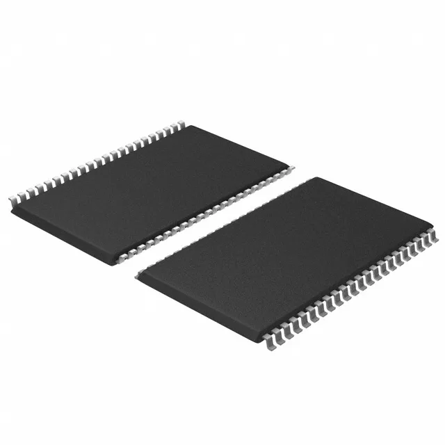
Housed in a 44-TSOP II (10.16 mm body width), this is a surface-mount package with a 0.8 mm pin pitch. The footprint is standard across the 4 Mbit async SRAM family — the same board layout works for the 3.3V variant and the tape-and-reel version (CY7C1041G-10ZSXIT). The tray shipment (25 pieces per tray) is typical for engineering samples and low-volume production; for higher volumes the tape-and-reel option avoids manual placement.