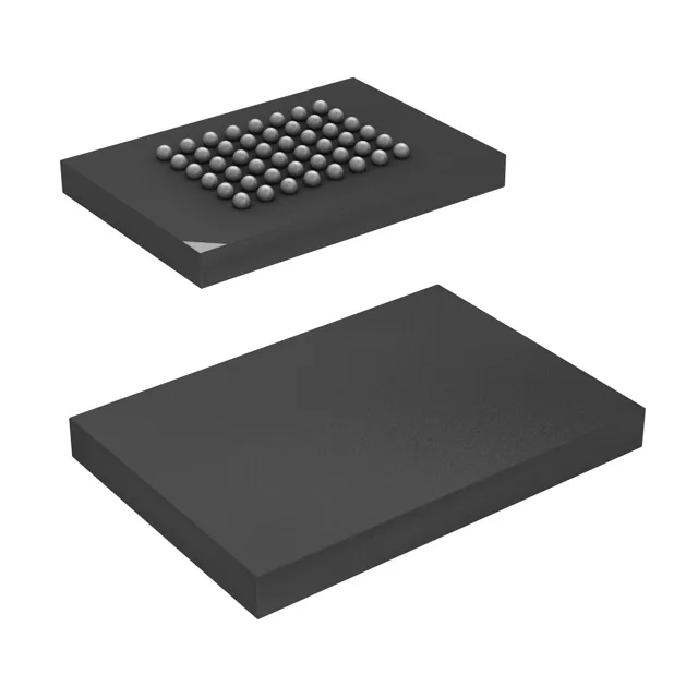
12 ns asynchronous SRAM in a 48-ball BGA
The CY7C1041CV33-12BAXET is a 4 Mbit asynchronous SRAM organized as 256K x 16 bits, with a 12 ns access time that sets the bus timing ceiling for the memory controller. The parallel interface means the address and data buses connect directly to a processor or FPGA without a serialization delay — the 12 ns cycle time keeps the read/write window tight enough for a 66 MHz bus with moderate trace lengths.
48-TFBGA footprint and board layout
Housed in a 48-ball TFBGA measuring 7 x 8.5 mm (supplier device package 48-FBGA), the ball pitch is 0.8 mm — a 4-layer board with microvias can fan out the inner rows without blind vias. The 0.8 mm pitch also means a standard BGA rework station with a 10 mm nozzle can handle it. The 256K x 16 organization uses 16 data lines and 18 address lines, so the PCB trace count is manageable for a mid-complexity memory bus.