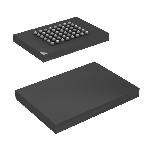
48-TFBGA footprint and board-fit
The CY7C1041CV33-10BAXET: The 0.5 mm pitch also sets the soldermask registration tolerance; a 0.25 mm solder-mask-defined pad with a 0.3 mm NSMD (non-solder-mask-defined) opening is the standard land pattern. If the reel has been opened longer than that, a 24-hour bake at 125°C before reflow is required to prevent popcorning.
10 ns access — what it means for the bus
The 10 ns access time sets the fastest read-cycle the memory can deliver — a 100 MHz bus with a 10 ns period leaves zero margin for address-to-data propagation when the memory controller's output delay and board trace flight time are added. For a 66 MHz bus (15 ns period), the 10 ns access leaves 5 ns for address hold, board delay, and setup at the controller, which is workable with careful layout. The 256K x 16 organization means the part presents a 16-bit word on each access — no byte-lane multiplexing or two-cycle read needed for a 16-bit data bus. This matches the external bus width of most ARM Cortex-M and ColdFire processors directly, saving a glue-logic latch.
Industrial temperature range and supply rail
The core and I/O share the same voltage, which simplifies the power tree but means the input thresholds track the supply; at 3.0V the VIH minimum is approximately 2.0V, so a 1.8V-logic MCU needs a level translator on the address/control lines.