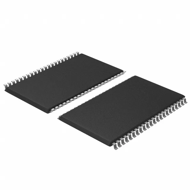
The CY7C1021CV33-12ZXIT is a 1Mbit asynchronous SRAM organized as 64K words by 16 bits, with a 12 ns access time. The 64K x 16 organization maps directly to 16-bit data buses found in many MCUs, DSPs, and FPGAs — no byte-lane steering logic needed. The 12 ns access time suits moderate-speed processor interfaces and glue-logic applications. Housed in a 44-TSOP II (0.400-inch body, 10.16 mm width) surface-mount package, it is a common footprint shared across several SRAM families, making board layout straightforward if a drop-in replacement is needed later.
Obsolete — planning your BOM line
Infineon lists this part as Obsolete. The 44-TSOP II footprint is widely used — many 1Mbit asynchronous SRAMs from other vendors share the same pinout and package. A cross-reference search against the 64K x 16, 12 ns, 3.3 V, 44-TSOP II profile will yield candidates, though each must be verified for timing and supply tolerance.
Access time and bus timing margin
In a system with a 66 MHz bus (15 ns period), this leaves only 3 ns of margin for address decoding, PCB trace delay, and setup time at the processor — tight but workable with careful layout. Write cycle time is also 12 ns, so the part can sustain back-to-back writes at the same speed. If your system runs a faster clock, look for a 10 ns or 8 ns variant in the same family.
The industrial temperature grade also provides margin in poorly ventilated designs where internal ambient rises above 70°C.