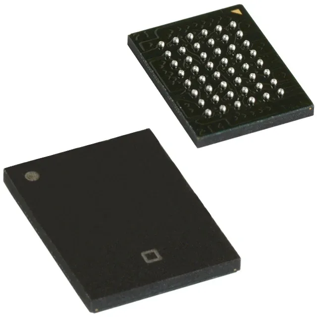
1Mbit asynchronous SRAM with 15 ns access — bus timing for 2.5V systems
The 15 ns access time means a bus master running at 66 MHz can complete a read cycle in one clock with zero wait states, assuming the address-to-data path stays within the timing budget. At higher clock rates, the 15 ns window starts to consume multiple cycles, so check the memory controller's setup/hold requirements against the part's output hold time.
The 125°C ceiling means the part can sit next to a hot CPU or power stage without derating the access time — though the 15 ns spec is typically measured at 25°C, and at 125°C the internal timing margins tighten. Budget an extra 2–3 ns for temperature derating if the system runs at the upper end of the range.
48-VFBGA package — board-level considerations
Housed in a 48-ball VFBGA (6x8 mm), this part uses a fine-pitch BGA footprint (0.5 mm ball pitch typical). The package is not hand-solderable; it requires a solder-paste stencil, reflow oven, and X-ray inspection for void detection. The small 6x8 mm body saves board space versus a TSOP-II, but the BGA's hidden solder joints make rework difficult.
The CY7C1021CV26-15BAET is marked obsolete by Cypress (now Infineon). For new designs, consider a pin-compatible 3.3V asynchronous SRAM in the same 48-VFBGA footprint if the system can tolerate a higher supply — though the 2.5V–2.7V supply range is the defining voltage domain, so a 3.3V part would require level shifters on the data bus.