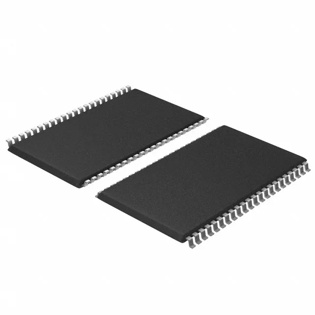
44-TSOP II footprint and 5V supply rail
The CY7C1021BN-15ZXCT: The tape-and-reel format suits high-volume pick-and-place; typical MSL for TSOP is level 3, so a bake before reflow is needed if the seal time has been exceeded. Do not connect to a 3.3 V memory bus without a level translator; the inputs are not 5 V tolerant at 3.3 V Vdd.
15 ns access time and 64K x 16 organization
Rated for 15 ns access time — this is the time from address valid to data valid on the bus. For a 16-bit MCU or MPU running at 40 MHz (25 ns cycle), the 15 ns access leaves 10 ns for address setup, hold, and board trace delay. The write cycle time is also 15 ns, so the bus controller must meet the write pulse width and data setup/hold windows within that window. The 64K x 16 organization matches a 16-bit data bus natively — no byte-lane steering needed for a 16-bit word, but 8-bit accesses require UB/LB control on the upper and lower byte enables. Asynchronous parallel SRAM means no clock, no refresh — the data is valid as long as power is applied and chip enable is asserted. The interface is simple glue logic (address, data, CE, OE, WE), but the 44-pin TSOP consumes more board area and routing layers than a serial SRAM or a synchronous SRAM with a reduced pin count. For new designs, consider a 3.3 V synchronous SRAM or a serial SRAM in a smaller package to save board space and power.
The tape-and-reel format is the standard reel for this part; tray or tube quantities may also be available from surplus inventory.