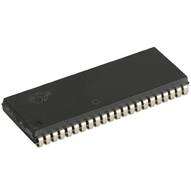
12 ns asynchronous SRAM for legacy 5V buses
It uses a parallel memory interface and comes in a 44-SOJ surface-mount package. This part is designed for high-speed cache, buffer, or scratchpad memory in systems that still run on a 5V rail — think legacy telecom line cards, industrial controllers, or test equipment that need fast, simple SRAM without clocked interfaces.
New designs should not target this order code. For existing BOM lines, the only viable channel is the independent distribution market — surplus, new-old-stock, or broker-sourced inventory.
The 12 ns access time is the chip-enable-to-data-valid window. In a 5V asynchronous system running at, say, 33 MHz (30 ns cycle), this leaves about 18 ns of margin for address decoding, board trace delay, and setup time at the receiving device. That is tight but workable for a single load on a short bus. If the system uses multiple SRAMs on the same data bus, the cumulative loading will stretch the access window — budget extra margin or use a slower cycle.
The 44-SOJ (Small Outline J-lead) package has a 0.400-inch body width (10.16 mm), surface-mount, with J-formed leads. This is a common footprint for 5V SRAMs of this density, but verify the land pattern against your PCB — SOJ-44 is not identical across all vendors. No industrial or automotive temperature variants are listed for this specific order code.