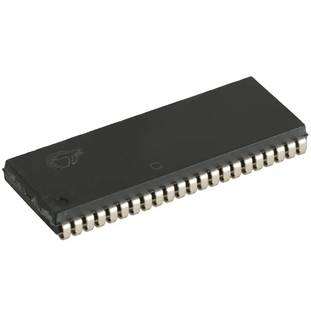
15 ns access time — timing closure for a 66 MHz bus
That 15 ns figure is the address-to-data valid delay; if your controller's memory interface has a 10 ns setup window, you've got 5 ns of PCB trace and clock jitter margin to work with. The 15 ns write cycle time matches the read cycle, so back-to-back transactions at 66 MHz are single-cycle — no dead bus turnaround.
If your BOM has already migrated to 3.3 V or lower, this SRAM needs a separate 5 V rail or a level translator on the address/data bus. The 44-SOJ package is a JEDEC-standard footprint shared with other 5 V asynchronous SRAMs of the same density, so a board layout swap to a different 64K x 16 5 V part is usually a drop-in — but not to a 3.3 V variant without a re-spin.
Obsolete — plan your BOM around surplus sourcing
Infineon (formerly Cypress) has ended production; there is no factory lead time, no last-time-buy window remaining. Any stock in the channel is new-old-stock or surplus inventory.
That rules out outdoor telecom cabinets, automotive under-hood, or any unheated industrial enclosure.