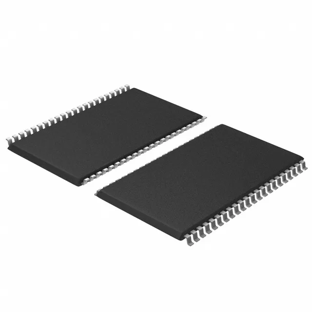
Infineon Technologies CY7C1020DV33-10ZSXIT — Memory (DRAM / SRAM / Flash / EEPROM)

Infineon CY7C1020DV33-10ZSXIT 512Kbit Async SRAM, 10 ns

MPNCY7C1020DV33-10ZSXIT
Active

Infineon CY7C1020DV33-10ZSXIT, 512Kbit Asynchronous SRAM (32K x 16), 10 ns access time, 3V to 3.6V supply, -40°C to 85°C industrial temperature, 44-TSOP II package, Tape & Reel.

$6.1800Ref. price · indicative, final on quote
Independent supplier — new & surplus stockAuthenticity-screened · ESD-safe packingListing updated Aug 2026

Specifications

CY7C1020DV33-10ZSXIT specifications
ParameterValue
Memory typeVolatile
MountingSurface Mount
Voltage3V ~ 3.6V
Memory interfaceParallel
Operating temperature-40°C ~ 85°C (TA)
PackageTape & Reel (TR) Cut Tape (CT)
TechnologySRAM - Asynchronous
Access time10 ns
Memory size512Kbit
Memory formatSRAM
Case44-TSOP (0.400\", 10.16mm Width)
Memory organization32K x 16
Write cycle time - word, page10ns

Product details

What this 512Kbit asynchronous SRAM brings to the bus

The Infineon CY7C1020DV33-10ZSXIT is a 512Kbit asynchronous SRAM organized as 32K x 16 bits, accessed through a parallel interface. Its 10 ns access time means a read or write cycle completes in one 100 MHz clock edge — no wait states for a 66 MHz bus, and only one wait for a 100 MHz bus. The 44-TSOP II package (0.400-inch body width, 10.16 mm) is a common footprint for 512Kbit parallel SRAMs, so board layout reuse across density upgrades is straightforward. The Tape & Reel shipping form is the standard for automated pick-and-place assembly lines.

10 ns access time — timing margin for the cache or buffer

For a DSP or MCU with a 66 MHz external bus, the 15 ns cycle budget leaves 5 ns of margin for PCB trace delay and clock skew — enough to avoid hold-time violations on a typical 2-layer board. If the bus runs at 100 MHz, the margin shrinks to zero, so the layout needs controlled impedance and matched trace lengths to keep setup times clean.

The base product number CY7C1020 covers multiple speed and temperature grades, so if a future spin needs a faster access time or a wider temperature range, the footprint stays the same.

Sourcing this part for a production line

If a design needs a wider temperature range or a different package, the CY7C1020 family has variants worth checking against the datasheet.

Frequently asked questions

What is the access time of CY7C1020DV33-10ZSXIT?

The access time is 10 ns for both read and write cycles (word, page). That lets it keep up with a 100 MHz bus without wait states, provided the PCB layout manages trace delay.

Is CY7C1020DV33-10ZSXIT a direct replacement for CY7C1020DV33-10ZSXI?

The suffix T in the order code indicates Tape & Reel packaging instead of tube or tray. Electrically and mechanically they are identical — same 10 ns access time, same 44-TSOP II footprint, same 3.3V supply and industrial temperature range. The T variant is simply the reeled version for automated assembly.

Is CY7C1020DV33-10ZSXIT a parallel SRAM?

Yes, it uses a parallel memory interface — address and data buses are separate, with chip enable, output enable, and write enable control lines. That is the standard interface for this 32K x 16 organization.