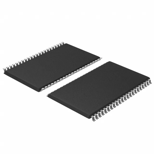
Infineon Technologies CY7C1020DV33-10ZSXI — Memory (DRAM / SRAM / Flash / EEPROM)

Infineon CY7C1020DV33-10ZSXI SRAM, 512Kbit, 10 ns

MPNCY7C1020DV33-10ZSXI
Active

Infineon CY7C1020DV33-10ZSXI, asynchronous SRAM, 512Kbit (32K x 16), 10 ns access time, parallel interface, 3V–3.6V supply, -40°C to 85°C, 44-TSOP II, tray.

$3.9040Ref. price · indicative, final on quote
Packaging44-TSOP (0.400", 10.16mm Width)
RoHSROHS3 Compliant
Independent supplier — new & surplus stockAuthenticity-screened · ESD-safe packingListing updated Aug 2026

Specifications

CY7C1020DV33-10ZSXI specifications
ParameterValue
Memory typeVolatile
MountingSurface Mount
Voltage3V ~ 3.6V
Memory interfaceParallel
Operating temperature-40°C~85°C(TA)
PackageTray
TechnologySRAM - Asynchronous
Access time10 ns
Memory size512Kbit
Memory formatSRAM
Case44-TSOP (0.400\", 10.16mm Width)
Memory organization32K x 16
Write cycle time - word, page10ns

Product details

This part is typically used as a fast scratchpad, cache buffer, or packet memory in networking gear, industrial controllers, and test equipment where deterministic, no-wait-state read/write cycles are required.

For a processor or DMA controller running at 50 MHz or less, this part delivers zero-wait-state performance without needing a synchronous burst mode.

32 K x 16 organization — why the 16-bit width matters

The 16-bit wide data bus matches 16-bit microcontrollers and DSPs directly, eliminating the need for byte-lane multiplexing or two-chip interleaving. This saves board area, reduces pin count on the controller side, and simplifies the PCB layout. For systems that need a 32-bit data path, two of these parts can be paired with shared address and control lines.

Package and rework: 44-TSOP II

The 44-TSOP II (0.400" body width, 10.16 mm) is a JEDEC-standard thin small-outline package with gull-wing leads. It is hand-reworkable with a hot-air station — the leads are visible for inspection and touch-up. The package is surface-mount and fits a common 44-pin TSOP II footprint.

It is RoHS3 compliant.

Frequently asked questions

Where can I buy CY7C1020DV33-10ZSXI?

This part is available to order through independent distribution. Submit an RFQ for current pricing and lead time confirmation.

What is the access time of CY7C1020DV33-10ZSXI?

The access time is 10 ns for both read and write cycles.

What is the memory organization of CY7C1020DV33-10ZSXI?

It is organized as 32 K words by 16 bits, giving a total of 512 Kbit.

What package does CY7C1020DV33-10ZSXI come in?

It is supplied in a 44-pin TSOP II package (0.400" body width, 10.16 mm), surface-mount, on tray.